
Semiconductor Wet Chemical Monitoring Applications
In the fast-evolving semiconductor industry, precision in chemical concentration measurement is critical to ensuring process stability, yield optimization, and cost efficiency.
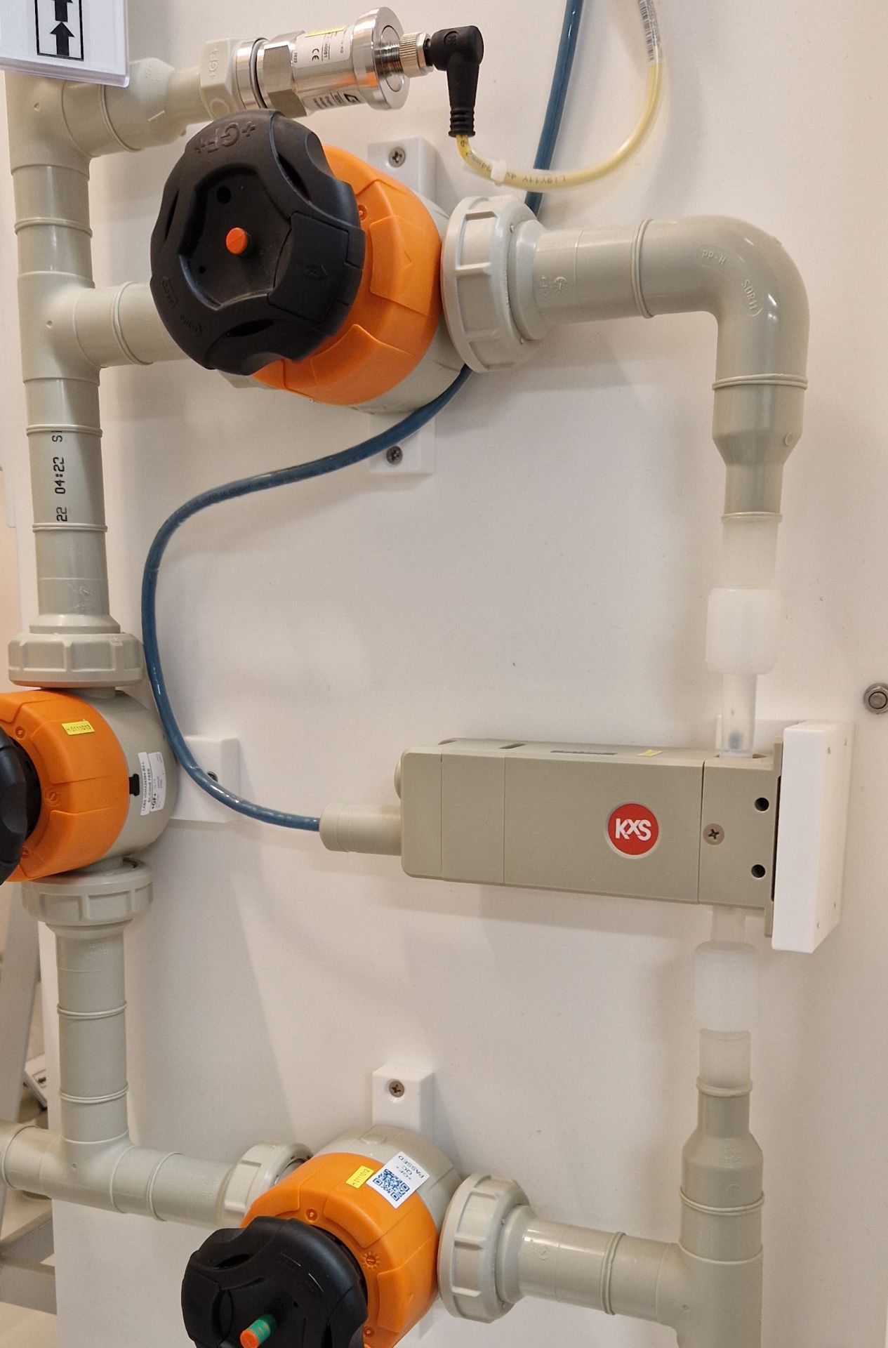
KxS Technologies’ in-situ refractive index measurement technology balances cost, speed and accuracy in providing real-time monitoring to maintain chemical integrity, reduce waste, and enhance process control throughout the fab distribution chain.
Typical application areas
1. Chemical blend checksum for SC-1 and SC-2
Our sensors are used in blender systems achieving the correct concentration of constituents in SC-1 and SC-2 cleaning solutions being essential for effective particle removal and surface preparation.
2. Onsite production of high-purity NH₃(aq) ammonium hydroxide
Along with an increasingly complex chemical supply chain new ways in generating chemicals onsite are advocated. Blenders generating bulk 29% NH₃(aq) from ammonia gas and water adopt the DCM-10 refractometer for ensuring the formation of ammonia liquid to its bulk concentration. Refractive index is uniquely a good match in the entire ammonia concentration range 0-30%wt.
3. Silicon wet etch with 50% KOH
Anisotropic wet etching of silicon with 50% potassium hydroxide (KOH) demands precise control to achieve smooth, accurate etching profiles, particularly in MEMS and deep etch applications.
4. Titanium etch with H₂SO₄:HNO₃:H₃PO₄ mixes
Titanium etching requires balanced acid blends of sulfuric acid (H₂SO₄), nitric acid (HNO₃), and phosphoric acid (H₃PO₄) to ensure efficient material removal while minimizing defects and over-etching. Our technology provides continuous monitoring for optimized concentration levels.
5. Backside poly etch with HF:HNO₃ mixtures
The selective etching of polycrystalline silicon on wafer back sides requires precise HF:HNO₃ concentration control to maintain process uniformity.
6. Post-CMP cleans with various mixtures
Chemical mechanical planarization (CMP) introduces contaminants that must be effectively removed using post-CMP cleaning solutions. Our sensors optimize cleaning bath life and ensure proper chemical balance for consistent wafer surface quality.
Why choose KxS for semiconductor applications?
- Real-time chemical monitoring – Instant concentration verification for process stability.
- Improved process yield – Reduce chemical waste and extend bath life.
- Cost and efficiency optimization – Minimize overuse of chemicals and improve ROI.
- Industry-proven reliability – Trusted by leading semiconductor fabs worldwide.
Find the best solution for your application
Our team of experts can help tailor the right monitoring solution for your specific semiconductor application.